Theme:
Program Counter & Branching
Create a new circuit
by adding a program counter to the circuit (+instructionDecoder-2022Spring.circ) from last week
Task
1:
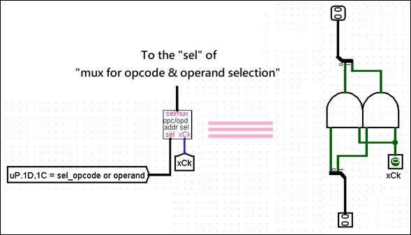
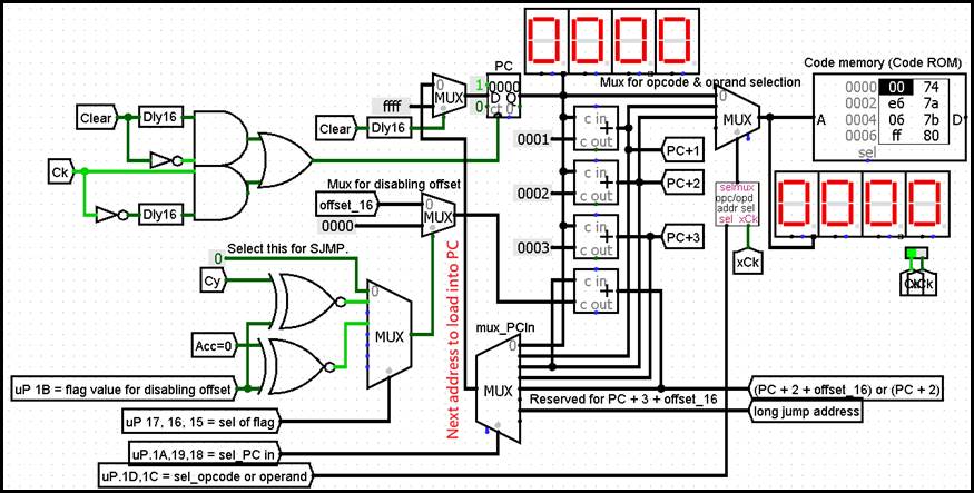
Connect
the Program Counter (PC) as in the
circuit shown below. (Note: The pink
ellipses indicate the new circuit part to be added in this week’s class.)
How to update the content of PC:
|
The initial value of the PC after it is cleared must be FFFF
so that its value will become 0000 when the first positive clock edge occurs.
|
In our CPU design, the PC never counts. Instead, it is constantly loaded on the rising clock
edge with one of the various values shown in the following table.
|
How to handle conditional/unconditional jumps:
|
For an unconditional branching
instruction (SJMP):
offset_16 0 000 PC+2+offset_16 |
||||||||
|
For a conditional branching
instruction resulting in branching:
001, etc. offset_16 0 PC+2+offset_16 |
||||||||
|
For a conditional branching
instruction resulting in no branching:
001, etc. 0000 1 PC+2+0000 |

How to control the fetching of the opcode and operands:
|
|
During the
positive CK half-cycle, PC is always selected as the address for the code
ROM. During the negative
CK half-cycle, PC + 1 or PC + 2 will be selected, and the selection is controlled
with “uP.1D,1C = sel_opcode or operand”. |
|||||||||||||||||||||||||||||||||||||||||
|
|
Task
2:
The
microprogram uses the following fields (Bit no. = 1DH ~ 15H) for program counter
control:
|
Bit no. (Hex) |
1F |
1E |
1D |
1C |
1B |
1A |
19 |
18 |
17 |
16 |
15 |
|
Bit no. (Decimal) |
31 |
30 |
29 |
28 |
27 |
26 |
25 |
24 |
23 |
22 |
21 |
|
mPM Addr |
|
|
Sel_ opcode or operand |
Flag
value for disabling offset |
sel PC in (= instru.
Length) |
Sel of flag |
|||||
In the microprogram template,
these fields of the microinstructions are empty. Please design these missing
bits.
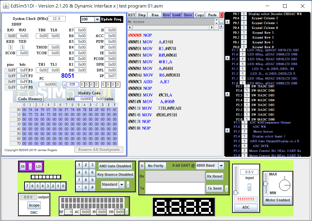
Test your design by
running the Test Program 01 shown
below.
This program is the
same as the test program in last week, except that it includes instructions, MOV direct,#imm, with 3-byte machine code (75
direct imm).
; Test Program
01 ¾ to
verify the functionality of the program counter
|
Assembly instruction |
Code ROM
Addr |
Machine
code |
minstruction address in mPM |
Execution Time, cycles |
Note |
|
|
|
NOP |
0000 |
00 |
00 |
1 |
|
|
|
MOV A,#24H |
0001 |
74 24 |
01 |
1 |
|
|
|
MOV R1,#07H |
0003 |
79 07 |
07 |
1 |
|
|
|
MOV R0,#06H |
0005 |
78 06 |
07 |
1 |
|
|
|
MOV @R1,A |
0007 |
F7 |
15, 16 |
2 |
(@R1) = (07) = 24. |
|
|
MOV A,#68H |
0008 |
74 68 |
01 |
1 |
|
|
|
MOV R6,#0DEH |
000A |
7E DE |
07 |
1 |
|
|
|
ADD A,R7 |
000C |
2F |
24 |
1 |
Acc = Acc + R7 = 68 + 24 = 8C. |
|
|
NOP |
000D |
00 |
00 |
1 |
|
|
|
MOV 0CH,A |
000E |
F5 0C |
0A |
1 |
(0C) = 8C. |
|
|
MOV A,@R0 |
0010 |
E6 |
04, 05 |
2 |
Acc = DE. |
|
|
MOV 72H,#0EAH |
0011 |
75
72 EA |
0B, oC |
2 |
This
is the first appearance of three-byte
machine code. |
|
|
MOV 0DH,#93H |
0014 |
75
0D 93 |
0B, 0C |
2 |
|
|
|
NOP |
0017 |
00 |
00 |
1 |
|
|
|
NOP |
0018 |
00 |
00 |
1 |
|
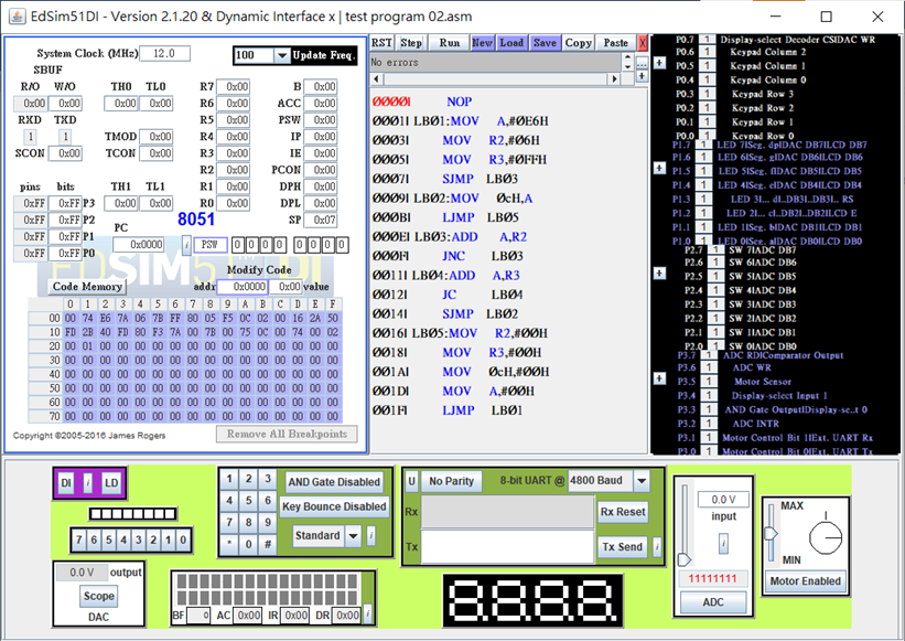
Task
3:
The microprogram
template also contains several branching instructions, including SJMP, LJMP,
JC, and JNC.
Please test them with
Test Program 02.
;
Test Program 02 ¾ to test the branching instructions
|
Assembly
instruction |
Code ROM
Addr |
Machine
code |
microinstruction address in mPM |
Execution Time, cycles |
Note |
|
|
|
NOP |
0000 |
00 |
00 |
1 |
|
|
|
|
|
|
|
|
|
|
LB01: |
MOV
A,#0E6H |
0001 |
74 E6 |
01 |
1 |
|
|
|
MOV
R2,#06H |
0003 |
7A 06 |
07 |
1 |
|
|
|
MOV
R3,#0FFH |
0005 |
7B FF |
07 |
1 |
|
|
|
SJMP LB03 |
0007 |
80 05 |
40 |
|
|
|
|
|
|
|
|
|
|
|
LB02: |
MOV
0cH,A |
0009 |
F5 0C |
0A |
1 |
Acc = FF è (0C) = FF. |
|
|
LJMP
LB05 |
000B |
02 00 16 |
42, 43 |
2 |
|
|
|
|
|
|
|
|
|
|
LB03: |
ADD
A,R2 |
000E |
2A |
24 |
1 |
Acc = E6, EC, F2, F8, FE, 04+C. |
|
|
JNC
LB03 |
000F |
50 FD |
46 |
1 |
|
|
|
|
|
|
|
|
|
|
LB04: |
ADD
A,R3 |
0011 |
2B |
04 |
Acc = 04+C, 03+C, 02+C, 01+C, 00+C, FF. |
|
|
|
JC
LB04 |
0012 |
40 FD |
44 |
1 |
|
|
|
|
|
|
|
|
|
|
|
SJMP
LB02 |
0014 |
80 F3 |
40 |
1 |
|
|
|
|
|
|
|
|
|
|
LB05: |
MOV
R2,#00H |
0016 |
7A 00 |
07 |
1 |
To reset the contents of the registers and
the RAM. |
|
|
MOV
R3,#00H |
0018 |
7B 00 |
07 |
1 |
|
|
|
MOV 0cH,#00H |
001A |
75 0C 00 |
0B, 0C |
2 |
|
|
MOV A,#00H |
001D |
74 00 |
01 |
1 |
|
|
|
|
LJMP
LB01 |
001F |
02 00 01 |
42, 43 |
2 |
|
|
|
|
|
|
|
|
|
Explanation
1:
Generation of the next instruction address,
to be loaded into the PC, for conditional/unconditional branching instructions:
|
Offset control ( For instruction with “uP. 1A, 19, 18, = sel PC in” = ’100’ or ‘101’) |
|||||||||
|
uP.
17, 16, 15 = Sel of flag |
000 |
001 |
010 |
011 |
100 |
101 |
Next address |
||
|
Flag
selected |
No
flag selected |
CY |
Bit |
Acc == 0 |
X – Y == 0 |
X – 1 == 0. X = X – 1 |
|||
|
Instruction |
uP 1B = Flag value for disabling offset |
||||||||
|
SJMP |
¾ |
|
|
|
|
|
PC + 2
+ offset |
||
|
LJMP |
¾ |
|
|
|
|
|
|
Long
jump address |
|
|
JC, |
0 |
|
CY =
0 |
|
|
|
|
PC +
2 |
|
|
CY =
1 |
PC +
2 + offset |
||||||||
|
JNC |
1 |
|
CY =
0 |
|
|
|
|
PC +
2 + offset |
|
|
CY =
1 |
|
|
|
|
PC +
2 |
||||
|
JB, |
0 |
|
|
Bit =
0 |
|
|
|
PC +
3 |
|
|
Bit =
1 |
PC +
3 + offset |
||||||||
|
JNB, |
1 |
|
|
Bit =
0 |
|
|
|
PC +
3 + offset |
|
|
Bit =
1 |
PC +
3 |
||||||||
|
JBC, |
0 |
|
|
Bit =
0 |
|
|
|
PC +
3 |
|
|
Bit =
1 |
PC +
3 + offset |
||||||||
|
---------- |
|
|
|
|
|
|
|
|
|
|
JZ, |
0 |
|
|
|
0
(Acc ¹ 0) |
|
|
PC + 2 |
|
|
1
(Acc == 0) |
PC +
2 + offset |
||||||||
|
JNZ |
1 |
|
|
|
0
(Acc ¹ 0) |
|
|
PC +
2 + offset |
|
|
1
(Acc == 0) |
PC +
2 |
||||||||
|
CJNE |
1 |
|
|
|
|
0 (x –
y ¹ 0) |
|
PC +
3 + offset |
|
|
1 ( X
– Y ==
0) |
PC +
3 |
||||||||
|
DJNZ |
1 |
|
|
|
|
|
0 (x
– 1 ¹ 0) |
PC +
3 + offset |
|
|
1 (X
– 1 == 0) |
PC +
3 |
||||||||
|
|
Yellow
background means that the instruction has been implemented in the week’s
circuit. |
|
|
|
|
|
|
|
|